 1 / 2
1 / 2
Project Overview
⚡ Proteus 8 Simulation — ECD Lab Project
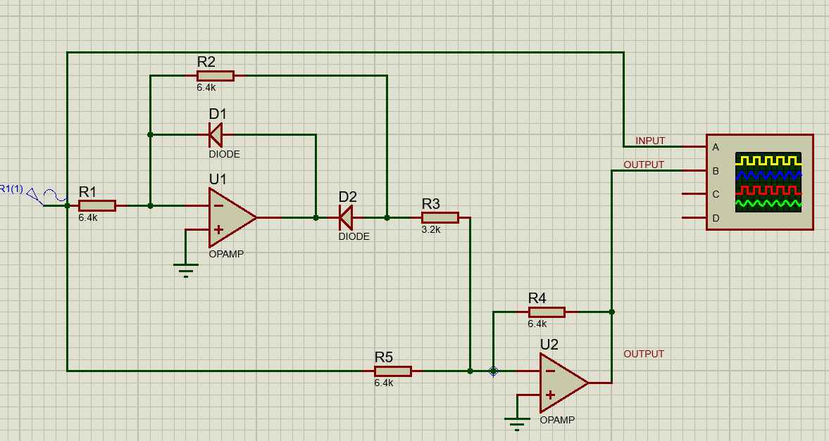
Full Wave Precision Rectifier
Op-Amp + Diode Circuit
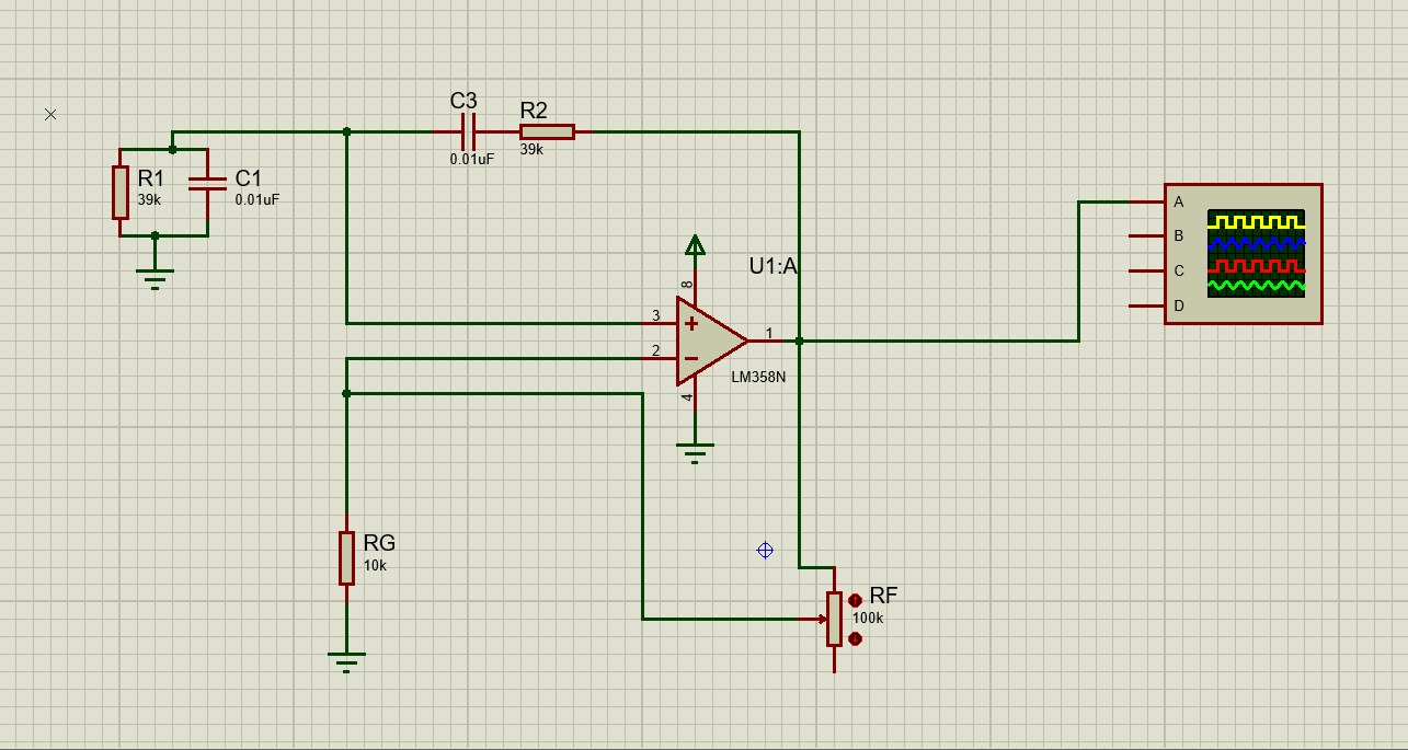
A dual op-amp precision rectifier that eliminates the 0.7V diode drop, enabling accurate rectification of signals as small as a few millivolts — verified on the Proteus digital oscilloscope.
Proteus 8
2× Op-Amp
Full Wave
Analog Electronics
Simulated ✓
📌 Overview
Unlike a conventional diode rectifier that suffers from a ~0.7V forward voltage drop, this precision rectifier places the diode inside the op-amp feedback loop — forcing the op-amp to automatically compensate for the drop. The result is an ideal diode with effectively 0V threshold, capable of rectifying any AC signal regardless of amplitude. The circuit uses two op-amp stages: an inverting half-wave rectifier followed by a summing amplifier to reconstruct the full-wave output.
Feature
Conventional
Precision
Min. Input Voltage
~0.7V
Near 0V
Forward Drop
0.7V per diode
~0V (compensated)
Accuracy
Low for small signals
High across all levels
Use Case
Power supplies
Instrumentation
⚡ Theory of Operation
Stage 1 — U1 (Inverting HW Rectifier)
- U1 configured as inverting amplifier
- D1 conducts on negative half-cycles via R2
- D2 blocks during positive half-cycles
- Output: inverted negatives → now positive
Stage 2 — U2 (Summing Amplifier)
- Sums Stage 1 output with original input
- R3, R4, R5 set weighted gains
- R4/R3 = 2 for correct amplitude scaling
- Result: full-wave rectified sine at output
// Stage 1 Gain (Inverting)
A₁ = −(R2 / R1) = −(6.4k / 6.4k) = −1
// Stage 2 Output (Summing Amplifier)
V_out = −[ (R4/R3) × V_stage1 + (R4/R5) × V_in ]
V_out = −[ 2 × V_stage1 + 1 × V_in ]
// Why R3 = 3.2kΩ (half of others)
R4 / R3 = 6.4k / 3.2k = 2 ← scales negative cycles correctly
🔧 Components
| Ref | Component | Value | Role |
|---|---|---|---|
| U1 | Op-Amp | — | Inverting half-wave rectifier stage |
| U2 | Op-Amp | — | Summing amplifier stage |
| D1 | Diode | — | Feedback diode — negative half-cycle path |
| D2 | Diode | — | Output diode — positive half-cycle path |
| R1 | Resistor | 6.4 kΩ | Input resistor |
| R2 | Resistor | 6.4 kΩ | Feedback resistor (Stage 1) |
| R3 | Resistor | 3.2 kΩ | Input resistor — Stage 2 (sets ×2 gain) |
| R4 | Resistor | 6.4 kΩ | Feedback resistor (Stage 2) |
| R5 | Resistor | 6.4 kΩ | Summing resistor (Stage 2) |
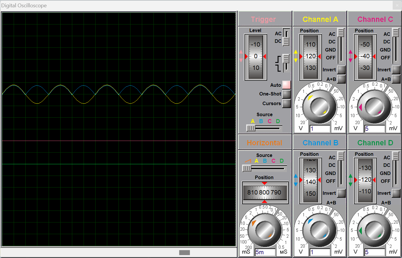
📊 Simulation Results
- ✅Channel A (Yellow) — Original AC sine wave input
- ✅Channel B (Blue) — Full wave rectified output
- ✅Both negative half-cycles correctly flipped to positive
- ✅No 0.7V diode drop visible — precision rectification confirmed
- ✅Stable, consistent waveform across all cycles
🔁 Half Wave vs Full Wave Precision Rectifier
| Feature | Half Wave | Full Wave |
|---|---|---|
| Rectified cycles | Positive only | Both +ve & −ve |
| Output ripple | High | Low |
| Efficiency | 50% | 100% |
| Op-Amps required | 1 | 2 |
| This project | ✗ | ✓ |
🌍 Real-World Applications
Audio Processing
Envelope detection and signal conditioning
Biomedical
ECG & EMG signal rectification
Power Metering
AC measurement & RMS conversion
Demodulation
Signal demodulation in comms systems
Instrumentation
Precision AC measurement in DMMs
DSP Input
Pre-processing before ADC conversion
📚 Key Concepts Covered
Ideal Diode Model
Op-Amp Feedback
Inverting Amplifier
Summing Amplifier
Weighted Resistor Network
Half-Wave Rectification
Full-Wave Rectification
Resistor Gain Ratio
Proteus Simulation
Virtual Oscilloscope
Signal Conditioning
Analog Circuit Design
Tech Stack
Proteus
Op-Amps
Analog Signal Processing
Circuit Simulation
Tags
Technical Specs
| Topology | Precision Full-Wave Rectifier / Absolute Value Circuit |
| Op-Amps | 2x Generic / Ideal Op-Amps (U1, U2) |
| Diodes | 2x Standard Rectifier Diodes (D1, D2) |
| Input Resistors | 6.4kΩ (R1, R5) |
| Feedback Resistors | 6.4kΩ (R2, R4) |
| Summing Resistor | 3.2kΩ (R3) - Sets gain of 2 |
| Simulation Software | Proteus 8 Professional |