 1 / 4
1 / 4
Project Overview
Square Wave Generator of Variable Frequency Using NE555 Timer
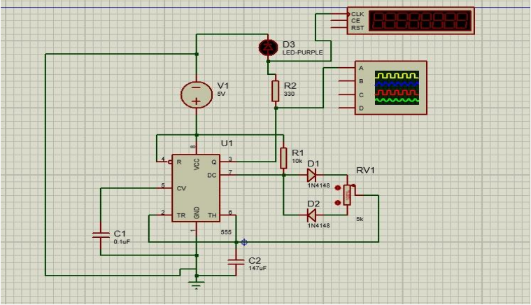
The objective of this project is to design and simulate a variable frequency square wave generator using the NE555 Timer IC configured in astable mode. The system demonstrates the fundamentals of hardware timing circuits and wave-shaping techniques.
A potentiometer is utilized to adjust the oscillation frequency of the circuit dynamically. An LED is connected directly at the output terminal to provide visual verification of the generated square waveform.
Circuit Description & Working Process
The NE555 timer is configured in astable multivibrator mode, meaning it continuously toggles between states and generates square waves without requiring an external triggering signal.
- Charging Phase: The timing capacitor C1 charges through R1 and R2. As the voltage across the capacitor rises from 1/3 Vcc to 2/3 Vcc, the output at Pin 3 becomes HIGH and the LED turns ON.
- Discharging Phase: When the capacitor voltage reaches 2/3 Vcc, the internal discharge transistor turns ON. The capacitor discharges back down to 1/3 Vcc through R2 only, forcing the output LOW and turning the LED OFF.
- Frequency Control: Adjusting the potentiometer (R2) changes the resistance in the timing network, shifting the charge/discharge durations and controlling the oscillation frequency.
- Noise Prevention: A 0.1 μF capacitor is connected to Pin 5 (Control Voltage) to stabilize the internal comparator reference levels against electrical noise.
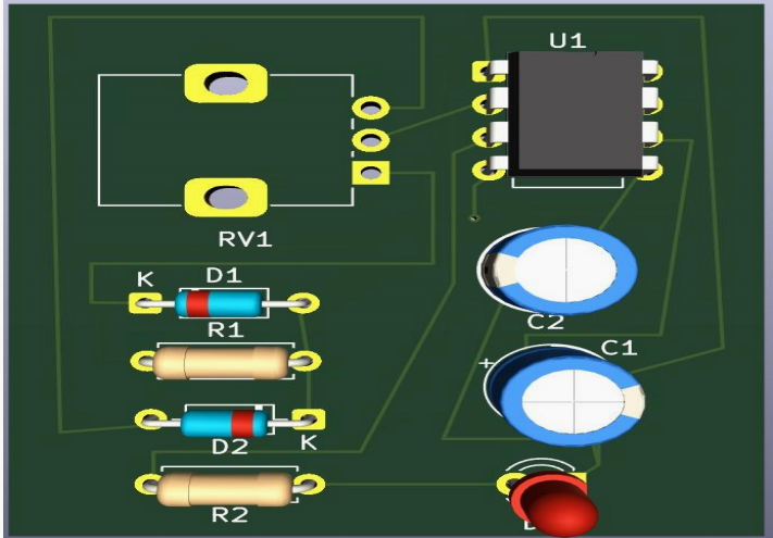
Equipment & Component Specifications
| Component | Value / Specification | Purpose |
|---|---|---|
| NE555 Timer IC | DIP-8 Package | Main multivibrator pulse generator |
| Potentiometer (R2) | 5 kΩ Variable | Dynamic frequency tuning control |
| Fixed Resistor (R1) | 10 kΩ | Sets baseline charging timing state |
| Timing Capacitor (C1) | 147 μF (100 μF || 47 μF) | Main charge reservoir for low-freq timing |
| Control Capacitor | 0.1 μF Ceramic | Pin 5 bypass decoupling filter |
| Output Indicators | Red LED + 330 Ω Resistor | Visual output state tracker & current limit |
| Diodes | 1N4148 (×2) | Waveform isolation shaping & protection |
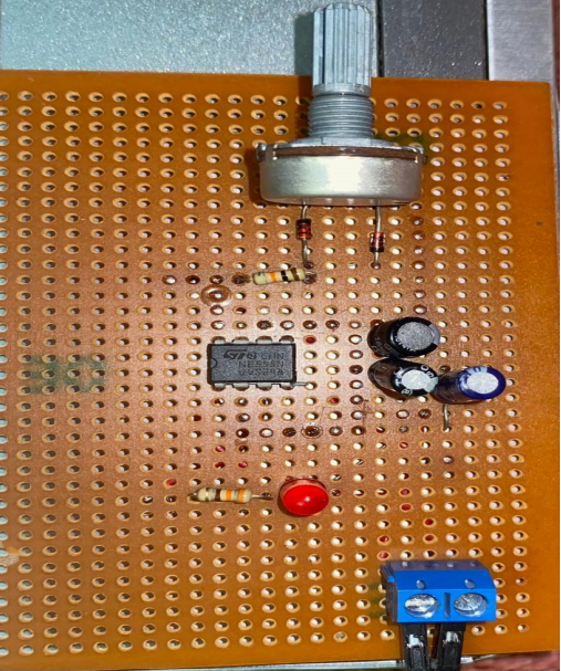
| Prototyping Hardware | Vero Board, Wires, 5-12 V DC Supply | Physical assembly environment and power |
Mathematical Calculations
The overall period (T) for the NE555 timer configured in astable mode is modeled using the classical equation:
Constants: R1 = 10 kΩ, C1 = 147 μF
T = 0.693 × (10,000 + 2 × 5,000) × (147 × 10-6)
T = 0.693 × (20,000) × (147 × 10-6)
T ≈ 2.038 seconds
T = 0.693 × (10,000 + 0) × (147 × 10-6)
T = 0.693 × (10,000) × (147 × 10-6)
T ≈ 1.02 seconds
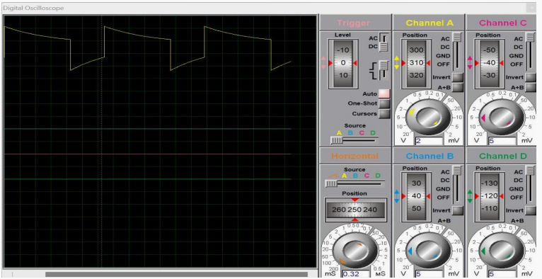
Observations & Visual Artifact Trait Explanations
When R2 hits 0 Ω, the total cycle length drops to ≈ 1.02s. However, the discharging duration transitions near instantaneous (0s). Because alternating intervals shift past the human eye's refresh rate threshold, persistence of vision merges the frames, causing the LED to appear steady.
- At maximum potentiometer value, the system delivers distinct blink intervals tracking at 1s active and 1s idle.
- At minimum resistance boundaries, frequency jumps higher, verifying that frequency is inversely proportional to control network resistance elements.
Hardware Module Connections & Application Scope
Applications Deployment Scope: Clock Signal Generators • Digital Pulse Processing Systems • LED Flasher Drivers • Embedded Instrumentation Timing Networks
Tech Stack
Tags
| Main IC | NE555 Timer IC (DIP-8) |
| Configuration | Astable Multivibrator Mode |
| Power Supply | 5–12V DC |
| Timing Capacitor (C1) | 147 µF (100 µF ∥ 47 µF) |
| Control Capacitor | 0.1 µF (Noise Filtering at Pin 5) |
| Resistor (R1) | 10 kΩ |
| Potentiometer (R2) | 5 kΩ (Variable Frequency Control) |
| Output Indicator | Red LED with 330 Ω Current Limiting Resistor |
| Waveform Shaping | 1N4148 Diodes (x2) |
| Assembly | Vero Board |