 1 / 6
1 / 6
Project Overview
⚡ Project Overview
A precision peak detector circuit fully simulated in Proteus Design Suite, using a real .wav audio file as the noise input source to generate continuously varying and unpredictable signal amplitudes — closely mimicking real-world electronic signal conditions. The circuit captures, tracks, and firmly holds the positive peak voltage of the input signal with high precision. This project demonstrates four progressive circuit designs, evolving from a basic diode-capacitor model all the way to a fully improved anti-saturation precision peak detector with buffer stage. Every design decision is backed by real simulation results observed on a 4-channel virtual oscilloscope within Proteus.
📌 What is a Peak Detector?
A peak detector is a fundamental analog circuit that measures and permanently holds the maximum voltage level reached by an input signal. Once the circuit captures a peak, it stores that value until a new higher peak appears or the circuit is manually reset. Peak detectors are critically important in a wide range of engineering applications including audio envelope detection, RF power measurement, vibration monitoring, medical ECG analysis, and industrial data acquisition systems. The operating principle is straightforward — when the input rises above the currently stored value, the capacitor charges to the new peak; when the input falls, the capacitor holds the last recorded maximum voltage indefinitely until reset.
🔁 Circuit Variants Implemented
① Simple Diode-Capacitor Peak Detector
The most fundamental and elementary form of peak detection, built using only a single diode and a single capacitor. When the input voltage rises above the voltage already stored on the capacitor, the diode becomes forward-biased and conducts, allowing the capacitor to charge up to the new peak voltage through the diode. Once the input starts to fall below this peak, the diode becomes reverse-biased and stops conducting entirely. At this point, the capacitor has no discharge path and holds the stored peak voltage steadily. The diode will only conduct again when the input voltage surpasses the previously stored peak, at which point the capacitor charges up to the new higher peak value and the cycle continues. This circuit is excellent for quick rough estimations but has one major limitation — a real silicon diode introduces a forward voltage drop of approximately 0.7 volts, which means the output voltage will always read slightly less than the true peak of the input. To detect the negative peak of the signal instead of the positive peak, simply reverse the direction of the diode in the circuit.
② Precision Peak Detector (Op-Amp + Diode)
To completely eliminate the diode forward voltage drop error that affects the simple circuit, a precision rectifier — also widely known as a super diode — is used in place of the ordinary diode. In a precision rectifier, the diode is placed inside the negative feedback loop of an operational amplifier. Because of the extremely high open-loop gain of the op-amp and the virtual ground principle, the op-amp automatically compensates for the 0.7V forward voltage drop of the diode by driving its output slightly higher to ensure the output node remains perfectly accurate. The resulting circuit behaves exactly like a mathematically ideal diode with absolutely zero forward voltage drop. By simply connecting a hold capacitor at the output terminal of this precision rectifier, we obtain a precision peak detector that captures the true and accurate peak of the input signal without any offset error or voltage loss. This is the preferred circuit wherever accurate peak measurements are required.
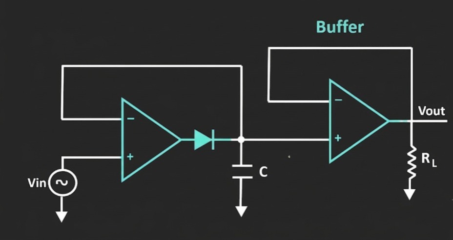
③ Buffered Peak Detector
In any real-world application, the output of the peak detector must be connected to some form of load — whether an external resistor, the input stage of another circuit block, or the input impedance of a data acquisition system or microcontroller ADC. The moment a load is connected, the hold capacitor begins to slowly discharge through that load resistance whenever the diode is reverse-biased and not conducting. This gradual discharge causes the stored peak voltage to droop over time, introducing serious measurement errors, especially for signals with longer time periods or when the load resistance is relatively small. The solution to this problem is to insert a buffer stage — a unity-gain voltage follower op-amp — between the hold capacitor and the load. The buffer presents an extremely high input impedance to the capacitor side, effectively acting as an open circuit and completely preventing the capacitor from discharging through the load resistance. At the same time, the buffer presents a very low output impedance to the load side, ensuring the load always sees the correct peak voltage without affecting the capacitor. Additionally, a reset switch or transistor can be connected directly across the hold capacitor to manually or electronically discharge it whenever a new measurement cycle needs to begin. A microcontroller GPIO pin can drive this transistor to automate the reset process in timed measurement systems.
RC Time Constant Design Rules:
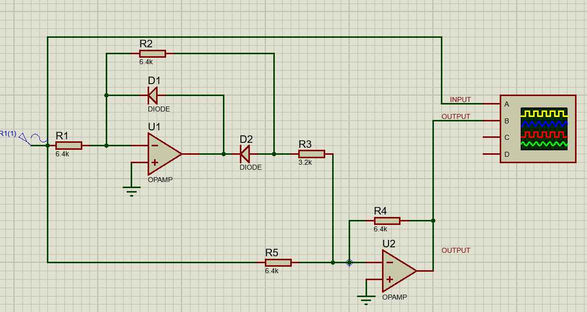
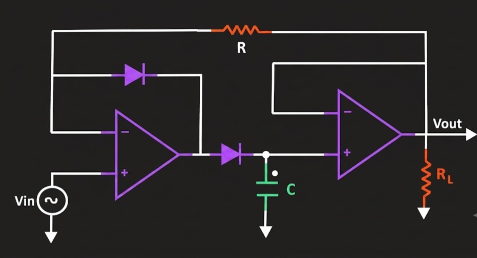
④ Improved Anti-Saturation Peak Detector
Even with the buffer stage solving the discharge problem, the buffered precision peak detector still suffers from one critical and fundamental flaw. When the diode is reverse-biased during the hold phase, the op-amp loses its feedback path entirely and begins operating in open-loop mode. In open-loop, even the tiniest difference between the input voltage and the stored peak voltage is amplified by the op-amp's enormous open-loop gain — typically over 100,000 — driving the op-amp output deep into negative saturation. When the input signal eventually rises above the stored peak again and the diode should begin conducting, the op-amp must first recover from deep saturation before it can respond. This recovery time is determined by the slew rate of the op-amp and can be significant, especially at higher signal frequencies. This saturation-recovery delay severely limits the maximum frequency of input signals that the circuit can accurately track and detect.
The improved design solves this completely by adding a second diode (D2) in a local feedback path directly around the first op-amp, along with a resistor R in the outer feedback loop. When the input drops below the stored peak and D1 becomes reverse-biased, the op-amp output momentarily swings negative, which immediately forward-biases D2 and closes a local feedback loop around the op-amp. This local feedback clamps the op-amp output to a voltage very close to the input voltage, preventing the output from ever reaching deep negative saturation. The op-amp remains in its linear operating region at all times. When the input rises above the stored peak again, D1 immediately begins conducting and the capacitor charges to the new peak with virtually no delay. The entire circuit can now accurately track fast-changing and high-frequency signals that would completely defeat the earlier designs. For ultra-high-speed peak detection applications, Schottky diodes are strongly recommended over standard 1N4148 signal diodes because Schottky diodes have a significantly lower forward voltage drop and extremely fast reverse recovery time.
🔬 Simulation Setup in Proteus
The complete circuit was constructed and simulated in Proteus Design Suite. A real .wav audio file was connected as the input signal source through Proteus's built-in signal generator, producing a complex noise-like waveform with continuously varying, unpredictable amplitudes across a wide range — closely simulating the kind of real-world signal a peak detector would encounter in practice. A 4-channel virtual oscilloscope was connected across key nodes of the circuit to simultaneously monitor the raw input waveform and the peak detector output voltage in real time, allowing direct visual comparison of circuit behavior.
Schematic Components:
Oscilloscope Channel Mapping:
📊 Oscilloscope Results & Observations
The oscilloscope output clearly and visually confirms the correct operation of the peak detector circuit. The yellow Channel A trace displays the raw audio noise input waveform with constantly varying, irregular amplitudes — exactly as expected from a real .wav audio source. The red Channel C trace shows the peak detector output — a near-flat DC level that rises in discrete steps each time a new higher amplitude peak is encountered in the input signal, and then very gradually and slowly decays between peaks due to minimal residual capacitor discharge through the buffer's finite input impedance. The buffer stage dramatically reduces this discharge rate compared to an unbuffered design. The circuit correctly and completely ignores all input voltage drops below the currently held peak value and updates the output only when a new maximum amplitude is detected. The results confirm that all four circuit variants perform as theoretically predicted.
⚙️ Key Design Considerations
🚀 Applications
👥 References
GenxiTechSolutions | amirrehman | soniaazhar
A precision peak detector circuit fully simulated in Proteus Design Suite, using a real .wav audio file as the noise input source to generate continuously varying and unpredictable signal amplitudes — closely mimicking real-world electronic signal conditions. The circuit captures, tracks, and firmly holds the positive peak voltage of the input signal with high precision. This project demonstrates four progressive circuit designs, evolving from a basic diode-capacitor model all the way to a fully improved anti-saturation precision peak detector with buffer stage. Every design decision is backed by real simulation results observed on a 4-channel virtual oscilloscope within Proteus.
📌 What is a Peak Detector?
A peak detector is a fundamental analog circuit that measures and permanently holds the maximum voltage level reached by an input signal. Once the circuit captures a peak, it stores that value until a new higher peak appears or the circuit is manually reset. Peak detectors are critically important in a wide range of engineering applications including audio envelope detection, RF power measurement, vibration monitoring, medical ECG analysis, and industrial data acquisition systems. The operating principle is straightforward — when the input rises above the currently stored value, the capacitor charges to the new peak; when the input falls, the capacitor holds the last recorded maximum voltage indefinitely until reset.
🔁 Circuit Variants Implemented
① Simple Diode-Capacitor Peak Detector
The most fundamental and elementary form of peak detection, built using only a single diode and a single capacitor. When the input voltage rises above the voltage already stored on the capacitor, the diode becomes forward-biased and conducts, allowing the capacitor to charge up to the new peak voltage through the diode. Once the input starts to fall below this peak, the diode becomes reverse-biased and stops conducting entirely. At this point, the capacitor has no discharge path and holds the stored peak voltage steadily. The diode will only conduct again when the input voltage surpasses the previously stored peak, at which point the capacitor charges up to the new higher peak value and the cycle continues. This circuit is excellent for quick rough estimations but has one major limitation — a real silicon diode introduces a forward voltage drop of approximately 0.7 volts, which means the output voltage will always read slightly less than the true peak of the input. To detect the negative peak of the signal instead of the positive peak, simply reverse the direction of the diode in the circuit.
② Precision Peak Detector (Op-Amp + Diode)
To completely eliminate the diode forward voltage drop error that affects the simple circuit, a precision rectifier — also widely known as a super diode — is used in place of the ordinary diode. In a precision rectifier, the diode is placed inside the negative feedback loop of an operational amplifier. Because of the extremely high open-loop gain of the op-amp and the virtual ground principle, the op-amp automatically compensates for the 0.7V forward voltage drop of the diode by driving its output slightly higher to ensure the output node remains perfectly accurate. The resulting circuit behaves exactly like a mathematically ideal diode with absolutely zero forward voltage drop. By simply connecting a hold capacitor at the output terminal of this precision rectifier, we obtain a precision peak detector that captures the true and accurate peak of the input signal without any offset error or voltage loss. This is the preferred circuit wherever accurate peak measurements are required.
③ Buffered Peak Detector
In any real-world application, the output of the peak detector must be connected to some form of load — whether an external resistor, the input stage of another circuit block, or the input impedance of a data acquisition system or microcontroller ADC. The moment a load is connected, the hold capacitor begins to slowly discharge through that load resistance whenever the diode is reverse-biased and not conducting. This gradual discharge causes the stored peak voltage to droop over time, introducing serious measurement errors, especially for signals with longer time periods or when the load resistance is relatively small. The solution to this problem is to insert a buffer stage — a unity-gain voltage follower op-amp — between the hold capacitor and the load. The buffer presents an extremely high input impedance to the capacitor side, effectively acting as an open circuit and completely preventing the capacitor from discharging through the load resistance. At the same time, the buffer presents a very low output impedance to the load side, ensuring the load always sees the correct peak voltage without affecting the capacitor. Additionally, a reset switch or transistor can be connected directly across the hold capacitor to manually or electronically discharge it whenever a new measurement cycle needs to begin. A microcontroller GPIO pin can drive this transistor to automate the reset process in timed measurement systems.
RC Time Constant Design Rules:
- Discharge condition (diode OFF): RC time constant must be at least 10 times greater than the time period of the input signal to minimize capacitor droop between peaks
- Charging condition (diode ON): RC time constant must be less than one-tenth of the signal time period so the capacitor charges rapidly and accurately to each new peak
- Note: Rd in the charging RC equation refers to the forward resistance of the conducting diode
④ Improved Anti-Saturation Peak Detector
Even with the buffer stage solving the discharge problem, the buffered precision peak detector still suffers from one critical and fundamental flaw. When the diode is reverse-biased during the hold phase, the op-amp loses its feedback path entirely and begins operating in open-loop mode. In open-loop, even the tiniest difference between the input voltage and the stored peak voltage is amplified by the op-amp's enormous open-loop gain — typically over 100,000 — driving the op-amp output deep into negative saturation. When the input signal eventually rises above the stored peak again and the diode should begin conducting, the op-amp must first recover from deep saturation before it can respond. This recovery time is determined by the slew rate of the op-amp and can be significant, especially at higher signal frequencies. This saturation-recovery delay severely limits the maximum frequency of input signals that the circuit can accurately track and detect.
The improved design solves this completely by adding a second diode (D2) in a local feedback path directly around the first op-amp, along with a resistor R in the outer feedback loop. When the input drops below the stored peak and D1 becomes reverse-biased, the op-amp output momentarily swings negative, which immediately forward-biases D2 and closes a local feedback loop around the op-amp. This local feedback clamps the op-amp output to a voltage very close to the input voltage, preventing the output from ever reaching deep negative saturation. The op-amp remains in its linear operating region at all times. When the input rises above the stored peak again, D1 immediately begins conducting and the capacitor charges to the new peak with virtually no delay. The entire circuit can now accurately track fast-changing and high-frequency signals that would completely defeat the earlier designs. For ultra-high-speed peak detection applications, Schottky diodes are strongly recommended over standard 1N4148 signal diodes because Schottky diodes have a significantly lower forward voltage drop and extremely fast reverse recovery time.
🔬 Simulation Setup in Proteus
The complete circuit was constructed and simulated in Proteus Design Suite. A real .wav audio file was connected as the input signal source through Proteus's built-in signal generator, producing a complex noise-like waveform with continuously varying, unpredictable amplitudes across a wide range — closely simulating the kind of real-world signal a peak detector would encounter in practice. A 4-channel virtual oscilloscope was connected across key nodes of the circuit to simultaneously monitor the raw input waveform and the peak detector output voltage in real time, allowing direct visual comparison of circuit behavior.
Schematic Components:
- U1 — Main Op-Amp: Primary amplifier driving the precision rectifier stage (LM741 / TL071 / OP07)
- U2 — Buffer Op-Amp: Unity-gain voltage follower isolating capacitor from load (LM741 / TL071)
- D1 — Main Diode: Primary signal diode for peak charging path (1N4148)
- D2 — Feedback Diode: Anti-saturation feedback diode preventing op-amp saturation (1N4148)
- R1 — Feedback Resistor: 10 kΩ in outer feedback loop
- RL — Load Resistor: 10 kΩ representing connected load at output
- C1 — Hold Capacitor: 10 µF electrolytic capacitor storing peak voltage
Oscilloscope Channel Mapping:
- Channel A (Yellow): Raw input signal from .wav noise generator — varying amplitude waveform
- Channel B (Blue): Input reference signal monitoring
- Channel C (Red): Peak detector output — slowly rising and holding DC level
- Channel D (Green): Additional circuit node monitoring
📊 Oscilloscope Results & Observations
The oscilloscope output clearly and visually confirms the correct operation of the peak detector circuit. The yellow Channel A trace displays the raw audio noise input waveform with constantly varying, irregular amplitudes — exactly as expected from a real .wav audio source. The red Channel C trace shows the peak detector output — a near-flat DC level that rises in discrete steps each time a new higher amplitude peak is encountered in the input signal, and then very gradually and slowly decays between peaks due to minimal residual capacitor discharge through the buffer's finite input impedance. The buffer stage dramatically reduces this discharge rate compared to an unbuffered design. The circuit correctly and completely ignores all input voltage drops below the currently held peak value and updates the output only when a new maximum amplitude is detected. The results confirm that all four circuit variants perform as theoretically predicted.
⚙️ Key Design Considerations
- Diode Voltage Drop: Standard silicon diodes introduce approximately 0.7V measurement error. Always use a precision rectifier op-amp circuit to eliminate this completely for accurate measurements.
- Capacitor Droop: Load resistance causes the hold capacitor to lose charge between peaks. Use a buffer op-amp to isolate the load and design the RC time constant to be at least 10 times the signal period.
- Op-Amp Saturation: Without feedback diode D2, the op-amp enters deep negative saturation during the hold phase. Saturation recovery time governed by slew rate severely limits maximum trackable signal frequency. The improved dual-diode design eliminates this completely.
- High-Speed Operation: For fast-changing signals, use Schottky diodes which have lower forward voltage (~0.2V) and dramatically faster switching and reverse recovery times compared to standard 1N4148 diodes.
- Op-Amp Selection: For high-frequency peak detection, choose op-amps with high slew rate and wide gain-bandwidth product such as TL071, LM318, or OP07 for precision applications.
- Circuit Reset: A mechanical switch or a transistor placed across the hold capacitor C1 allows the circuit to be reset and discharged on demand. A microcontroller GPIO pin can drive this transistor to fully automate cyclic measurements.
- Input Impedance: The buffer stage provides extremely high input impedance protecting the capacitor, while presenting very low output impedance to the load — ensuring accurate voltage transfer with no loading effect.
🚀 Applications
- Audio signal envelope detection and dynamic range measurement
- RF and microwave signal peak power measurement systems
- Industrial vibration and mechanical shock monitoring
- Battery and power supply peak voltage monitoring
- Industrial sensor and transducer data acquisition
- Automatic gain control (AGC) feedback circuits
- Medical instrumentation — ECG and biomedical peak detection
- Radar and sonar signal processing front-ends
- Motor drive and power electronics protection circuits
👥 References
GenxiTechSolutions | amirrehman | soniaazhar
Tech Stack
Proteus Design Suite
Op-Amp
1N4148 Diode
Capacitor
Resistor
Virtual Oscilloscope
WAV Signal Generator
Tags
Technical Specs
| Circuit Type | Precision Peak Detector |
| Simulation Tool | Proteus Design Suite |
| Input Source | .wav Audio File (Noise Generator) |
| Signal Type | Random Amplitude Noise Waveform |
| Hold Capacitor (C1) | 10 µF Electrolytic |
| Feedback Resistor (R1) | 10 kΩ |
| Load Resistor (RL) | 10 kΩ |
| Main Diode (D1) | 1N4148 Signal Diode |
| Feedback Diode (D2) | 1N4148 Signal Diode |
| Op-Amp U1 | Main Amplifier (LM741 / TL071) |
| Op-Amp U2 | Unity-Gain Buffer (LM741 / TL071) |
| Number of Op-Amps | 2 |
| Oscilloscope Channels Used | 4 |
| Channel A | Raw Input Signal (Yellow) |
| Channel B | Input Reference |
| Channel C | Peak Detector Output (Red) |
| Channel D | Additional Node Monitor |
| Diode Type (High Speed) | Schottky (recommended) |
| Forward Voltage Drop (1N4148) | ~0.7V |
| Precision Rectifier | Yes (Zero Voltage Drop) |
| Buffer Stage | Yes (High Input Impedance) |
| Anti-Saturation Design | Yes (Dual Diode D1 + D2) |
| RC Discharge Condition | RC ≥ 10 × Signal Period |
| RC Charging Condition | RC ≤ (1/10) × Signal Period |
| Peak Detection Type | Positive Peak |
| Reset Mechanism | Switch / Transistor across C1 |
| Category | Analog Electronics |
| Year | 2025 |